
Z-Wave Hardware Best Practices
Part 6: Z-Wave Hardware Best Practices, focuses on practical hardware design techniques for engineers developing low-cost, reliable Z-Wave IoT devices. It covers PCB layout recommendations, cost optimization, RF considerations, manufacturing best practices, and design guidelines drawn from real-world engineering experience.
Introduction
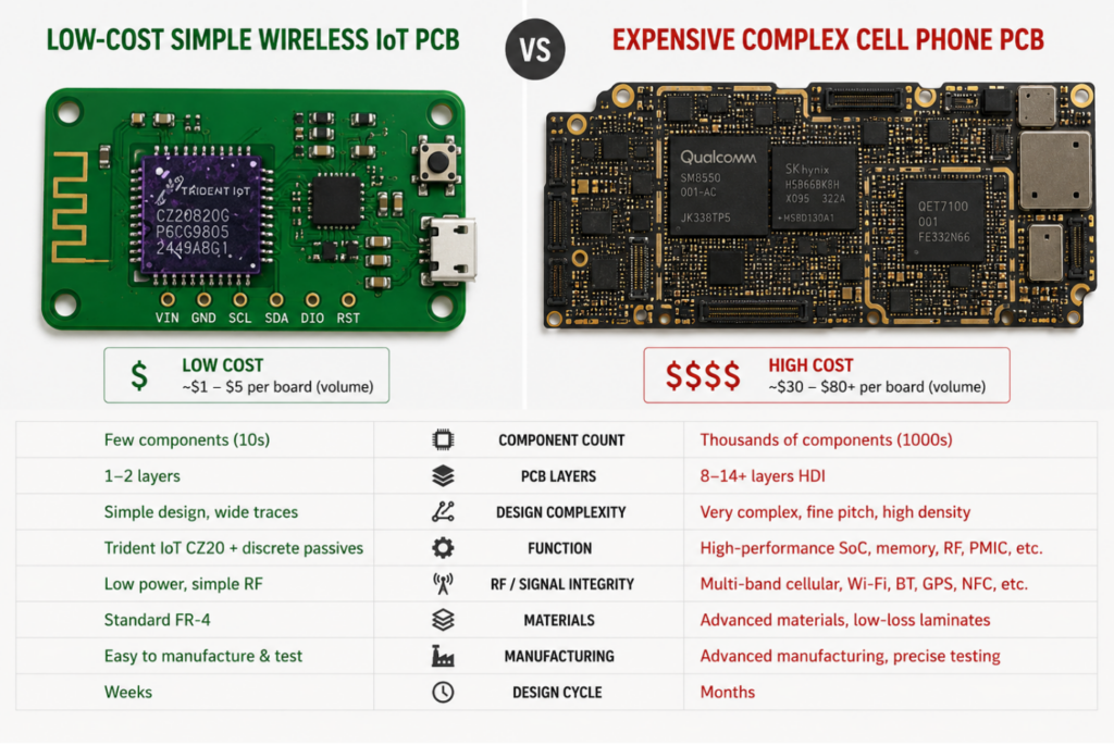
Cost sensitive wireless smart home devices have different requirements compared to designing cell phones or laptops. The printed circuit boards (PCB) are usually only a few square inches and often only two layers. To fit inside of an electrical outlet box the entire product must be small and cost considerations require integrated microcontrollers to supply most of marketings requirements.
Basics of IoT Device Hardware
Can AI design and layout a PCB? I recently tried one of the new AI PCB design tools with their free 14-day trial. I uploaded the ZRADmini schematic into the “free” version of the tools which ran out of ACUs (Agentic Compute Units) before it could even digest the library components. Maybe if I had paid for a subscription, I might be able to get something useful, but on my limited budget I didn’t spend more time or money trying the tool out. Low-cost IoT devices have simple, one-page schematics and small PCBs. Most of the effort is connecting the wireless MCU and designing the antenna. Both of which require expertise that comes from years of designing IoT products.
A key feature of having the engineer do the PCB design, is that the engineer can easily change the MCU pinout to solve PCB layout problems. Since both Silicon Labs and Tridents chips can route nearly any peripheral to almost any GPIO, I often swap GPIOs while routing the PCB. Make a quick change to the schematic, reread the netlist in the layout tool and voilà, problem solved! Just remember to also change the pinout in the firmware.
I usually manually design, layout and hand-assemble prototypes. If I need to build more than five, I contract assembly out because assembly quickly becomes a huge time sink. I use the open source KiCAD electronic design software. I have contributed a few library components to the repo including the Silicon Labs ZG23 and Tridents CZ20. Many PCB vendors can directly import KiCAD files, but I prefer to send them good ol’ Gerber files to ensure I get exactly what I want. With the KiCAD files, the vendor may adjust parameters such as the solder mask clearance which results in no solder mask between the fine pitch pins of the MCU resulting in nothing but solder shorts between the tiny pins. I don’t even use the autorouter as it tends to make a mess of things with way too many vias. The routing is usually simple enough to complete in a few hours and is an enjoyable game of close-the-rats-nets.
Keeping Costs Low
The main cost driver for consumer electronics is volume. The higher the annual volume, the lower the cost for nearly every line item; PCB manufacturing, the MCU, passives, ICs, assembly, test and packaging. If the product volume isn’t at least in the 10K units/year range, then it must be unique enough to command a high price. There is a significant knee-of-the-curve at the 10k threshold.
Don’t spend too much time checking, rechecking, and reviewing the schematic and layout. The turnaround time for a new prototype PCB can be as little as overnight, and the cost of a new board is just a few dollars. Thus, it makes sense to send the board out quickly and expect to spin it once or twice to fix a couple of errors. I accidentally put the wrong size passive component on the board and only discovered the mistake when it barely fits in the footprint on the board. But that’s easily fixed and a new board is ready next week. I’ve also reversed the pinout of a connector or some other special component that gives the bottom view in the datasheet instead of the top view. Again, easily fixed and I have new boards in about a week. Be careful with GPIO selection as the 800 series has limitations on power domain and wakeup capabilities of certain pins. See my GPIO blog for more details.
Rules For Low-cost IoT Products
Naturally these “rules” are not absolute requirements but instead are recommendations. Engineering is the art of balancing the solution to meet the requirements in a cost-efficient manner. Often it is worthwhile to push back on a requirement if the cost is too high so don’t simply accept the requirements as non-negotiable. The first rule here is an example of these engineering tradeoffs: a four-layer PCB is more expensive, but you get better impedance (thus better RF) and likely a smaller PCB. The balance between 2 vs. 4 layers is unique for every product which means it must be engineered.
- Minimize PCB layers
- 2 works for most Z-Wave designs
- 4 costs ~40% more for bare PCB but has better impedance/RF
- Minimize size
- PCB costs are computed by the square millimeter
- Remember the GND plane of the PCB is half of the antenna
- Rectangular outline
- Simple shape maximizes array utilization
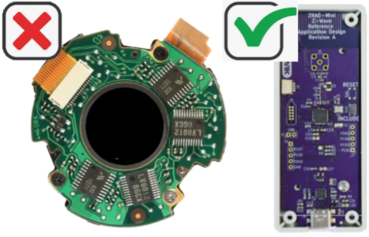
- Ideally v-scored for minimal waste
- Simple shape maximizes array utilization
- 0.16-0.20mm (6-8mil) wire spacing
- follow the design rules of the low-cost PCBs manufacturer
- Minimize special holes
- Slots, unusual sizes, edge features all cost $
- All SMT components on one side – cheaper, easier and higher yield
- 0402/0603 passive components with enough space for easy Pick&Place
- 0201s are the size of a grain of sand – difficult to manage
- Larger sizes cost more with no significant benefit
- Minimize manual assembly & soldering
- PCB cost is driven by turnaround time
- Waiting for an extra week is cheaper
PCB Design Recommendations
- Use the Mini Simplicity debug footprint
- Avoid custom footprints!
- Requires fragile & expensive jig for debug/production
- Use the standard Tag-Connect footprint & cable
- The spring post cable alignment pins enabling reliable programming and test
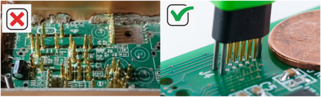 has
has - Ideally make the footprint visible under a battery door to allow (re)programming after the device has been inserted into the enclosure.
- Avoid custom footprints!
- No wires under the RF traces
- Ideally all RF traces are all on component side
- Minimize vias which are impedance discontinuities
- Surround with ground vias
- Use the vendor recommended crystals as they have been vetted by the vendor
- Continuous Ground fills
- Ideally have a continuous ground fill on the back for better RF
- Add thru-hole vias to the VCOM TX signal
- See when printfs are coming out on a scope compared to current consumption
- Can be done by making a via larger (1mm)
- Connect extra GPIOs to thru-hole test points
- Accessible from both sides of the PCB
- Easily prototype hardware changes or future features
- Add a hardware version GPIO Resistor Divider Pair or capacitor
- high ohms so little current
- Version 1=pulled up, Version 2=pulled down
- Version 3 onward uses the ADC to measure voltage or a cap and a timer
- Review the ground plane flood fills
- Ensure current paths do not require changing layers
- No antennas
- No floating areas
- Array vias between top and bottom
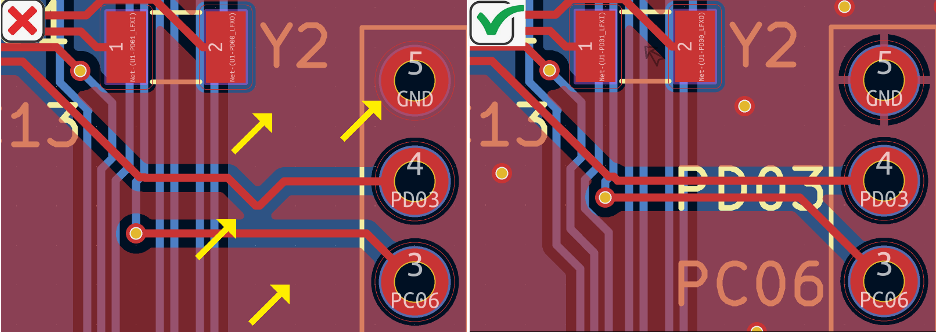
Figure 1 Can you identify the errors?
- Avoid wires under the Z-Wave chip
- The EP prevents this anyway
- Silkscreen signal names on connectors and test points
- All ground connections must have thermal reliefs
- WSTK has several pins flood filled to a thru-hole – nearly impossible to solder!
- Analog has special rules! Follow them!
- Have a checklist, follow it, add new items to avoid previous mistakes
- DRC rules must pass
- All nets routed
Resources
Here are a few links to suppliers I use or have used in the past. There are many PCB manufacturers and electronic assembly houses, thus it is likely there is one local to you. One rule I use to find local vendors is if they have tanks or planes or military hardware photos on their web site, they are not going to be cost competitive for IoT.
- Electronic Components
- PCB manufacturers
- OSHPark – my current Go-To for prototype PCBs
- PCB Unlimited
- Sunstone
- Stencil providers
- OSHStencils – linked with OSHPark
- The other PCB vendors can produce stencils from the Gerbers
- Assembly
- ScreamingCircuits – Full service from PCB to assembled prototypes
- You’ll send them the MCU and any uncommon components
- Seeed Studio – I buy their maker boards for GPS and displays but they also have a division for prototyping
- ScreamingCircuits – Full service from PCB to assembled prototypes
See my public ZRAD github repo for detailed procedures for going from schematics to PCB layout to assembling prototypes.
Next Steps
Part 7 of the Z-Wave Developer’s Journey discusses how to debug and optimize battery life. Matching the proper type of battery to the needs of your product and achieving the desired battery life requires classic engineering skills. I’ll go over a few tips from my years of optimizing coin cell battery devices to last for years. As we continue along the Z-Wave Developer’s Journey, I welcome your comments and questions. Please feel free to reach out to me directly via email.
About the Author
Eric Ryherd has been at the forefront of Z-Wave innovation since 2003, beginning as a consultant and later serving as a Field Application Engineer at Silicon Labs. Over the course of his career, he has contributed to the design and development of a wide range of Z-Wave products, including sensors, remote controls, motorized window shades, and in-wall dimmers, many of which are on the market today.
Although he “retired” in 2022, Eric remains deeply engaged in embedded systems and Z-Wave development through his blog, DrZWave.blog, and ongoing IoT consulting projects. He is also a familiar face at Z-Wave Alliance Unplug Fests, where he frequently serves as the lead coordinator, supporting interoperability and developer collaboration.
